- 您现在的位置:买卖IC网 > Sheet目录415 > FDB3860 (Fairchild Semiconductor)MOSFET N-CH 100V 6.4A D2PAK
�� �
�
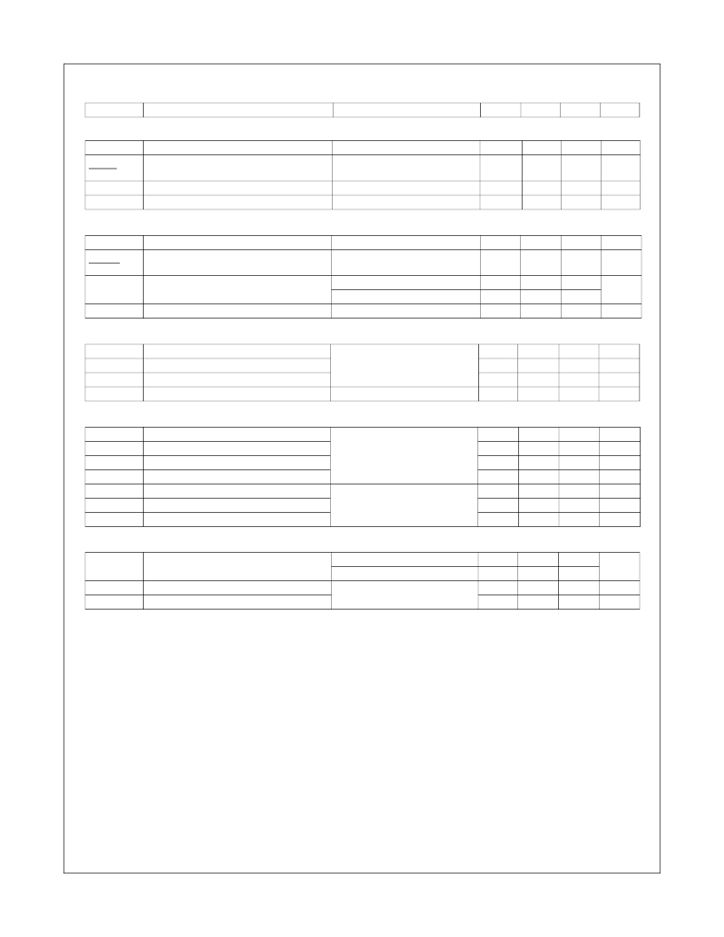
�Electrical� Characteristics� T� J� =� 25� °C� unless� otherwise� noted�
�Symbol�
�Parameter�
�Test� Conditions�
�Min�
�Typ�
�Max�
�Units�
�Off� Characteristics�
�BV� DSS�
�?� BV� DSS�
�?� T� J�
�I� DSS�
�I� GSS�
�Drain� to� Source� Breakdown� Voltage�
�Breakdown� Voltage� Temperature�
�Coefficient�
�Zero� Gate� Voltage� Drain� Current�
�Gate� to� Source� Leakage� Current�
�I� D� =� 250� μ� A,� V� GS� =� 0� V�
�I� D� =� 250� μ� A,� referenced� to� 25� °C�
�V� DS� =� 80� V,� V� GS� =� 0� V�
�V� GS� =� ±20� V,� V� DS� =� 0� V�
�100�
�104�
�1�
�±100�
�V�
�mV� /� °C�
�μ� A�
�nA�
�On� Characteristics�
�V� GS(th)�
�?� V� GS(th)�
�?� T� J�
�r� DS(on)�
�g� FS�
�Gate� to� Source� Threshold� Voltage�
�Gate� to� Source� Threshold� Voltage�
�Temperature� Coefficient�
�Static� Drain� to� Source� On� Resistance�
�Forward� Transconductance�
�V� GS� =� V� DS� ,� I� D� =� 250� μ� A�
�I� D� =� 250� μ� A,� referenced� to� 25� °C�
�V� GS� =� 10� V,� I� D� =� 5.9� A�
�V� GS� =� 10� V,� I� D� =� 5.9� A,� T� J� =� 125� °C�
�V� DS� =� 10� V,� I� D� =� 5.9� A�
�2.5�
�3.8�
�-11�
�31�
�56�
�18�
�4.5�
�37�
�67�
�V�
�mV/°C�
�m� ?�
�S�
�Dynamic� Characteristics�
�C� iss�
�C� oss�
�C� rss�
�R� g�
�Input� Capacitance�
�Output� Capacitance�
�Reverse� Transfer� Capacitance�
�Gate� Resistance�
�V� DS� =� 50� V,� V� GS� =� 0� V,�
�f� =� 1� MHz�
�1310�
�100�
�40�
�1.7�
�1740�
�130�
�65�
�pF�
�pF�
�pF�
�?�
�Switching� Characteristics�
�t� d(on)�
�Turn-On� Delay� Time�
�12�
�22�
�ns�
�t� r�
�t� d(off)�
�t� f�
�Q� g�
�Q� gs�
�Q� gd�
�Rise� Time�
�Turn-Off� Delay� Time�
�Fall� Time�
�Total� Gate� Charge� at� 10� V�
�Gate� to� Source� Charge�
�Gate� to� Drain� “Miller”� Charge�
�V� DD� =� 50� V,� I� D� =� 5.9� A,�
�V� GS� =� 10� V,� R� GEN� =� 6� ?�
�V� DD� =� 50� V,� I� D� =� 5.9� A�
�6�
�17�
�3�
�21�
�6.9�
�5.4�
�12�
�31�
�10�
�30�
�ns�
�ns�
�ns�
�nC�
�nC�
�nC�
�Drain-Source� Diode� Characteristics�
�V� SD�
�Source� to� Drain� Diode� Forward� Voltage�
�V� GS� =� 0� V,� I� S� =� 2.0� A�
�V� GS� =� 0� V,� I� S� =� 5.9� A�
�(Note� 2)�
�(Note� 2)�
�0.7�
�0.8�
�1.2�
�1.3�
�V�
�t� rr�
�Q� rr�
�Reverse� Recovery� Time�
�Reverse� Recovery� Charge�
�I� F� =� 5.9� A,� di/dt� =� 100� A/� μ� s�
�35�
�37�
�56�
�60�
�ns�
�nC�
�Notes� :�
�1:� R� θ� JA� is� the� sum� of� the� junction-to-case� and� case-to-ambient� thermal� resistance� where� the� case� thermal� reference� is� defined� as� the� solder� mounting� surface� of� the� drain� pins.�
�R� θ� JC� is� guaranteed� by� design� while� R� θ� JA� is� determined� by� the� user’s� board� design.�
�a� .� 40� °C/W� when� mounted� on� a� 1� in� 2� pad� of� 2� oz� copper�
�b� .� 62.5� °C/W� when� mounted� on� a� minimum� pad.�
�2:� Pulse� Test:� Pulse� Width� <� 30� 0� μ� s,� Duty� cycle� <� 2.0%.�
�3:� Starting� T� J� =� 25� °� C� ,� L� =� 3� mH� ,� I� AS� =� 8� A� ,� V� DD� =� 100� V� ,� V� GS� =� 10� V.�
�?2009� Fairchild� Semiconductor� Corporation�
�FDB3860� Rev� .� C�
�2�
�www.fairchildsemi.com�
�发布紧急采购,3分钟左右您将得到回复。
相关PDF资料
FDB390N15A
MOSFET N-CH 150V 27A D2PAK
FDB44N25TM
MOSFET N-CH 250V 44A D2PAK
FDB52N20TM
MOSFET N-CH 200V 52A D2PAK
FDB5800_F085
MOSFET N-CH 60V 80A D2PAK
FDB6030L
MOSFET N-CH 30V 48A D2PAK
FDB6670AL
MOSFET N-CH 30V 80A D2PAK
FDB8132
MOSFET N-CH 30V 80A D2PAK
FDB8160
MOSFET N-CH 30V 80A D2PAK
相关代理商/技术参数
FDB38N30U
功能描述:MOSFET N-Channel UniFETTM Ultra FRFETTM MOSFET 300V, 38A, 120m RoHS:否 制造商:STMicroelectronics 晶体管极性:N-Channel 汲极/源极击穿电压:650 V 闸/源击穿电压:25 V 漏极连续电流:130 A 电阻汲极/源极 RDS(导通):0.014 Ohms 配置:Single 最大工作温度: 安装风格:Through Hole 封装 / 箱体:Max247 封装:Tube
FDB390N15A
功能描述:MOSFET 150V NCHAN PwrTrench RoHS:否 制造商:STMicroelectronics 晶体管极性:N-Channel 汲极/源极击穿电压:650 V 闸/源击穿电压:25 V 漏极连续电流:130 A 电阻汲极/源极 RDS(导通):0.014 Ohms 配置:Single 最大工作温度: 安装风格:Through Hole 封装 / 箱体:Max247 封装:Tube
FDB-4
功能描述:化学物质 YELLOWCAP 10/PACK RoHS:否 制造商:3M Electronic Specialty 产品:Adhesives 类型:Epoxy Compound 大小:1.7 oz 外壳:Plastic Tube
FDB4020P
功能描述:MOSFET P-Ch Spec Enhance MODE FIELD EFFECT RoHS:否 制造商:STMicroelectronics 晶体管极性:N-Channel 汲极/源极击穿电压:650 V 闸/源击穿电压:25 V 漏极连续电流:130 A 电阻汲极/源极 RDS(导通):0.014 Ohms 配置:Single 最大工作温度: 安装风格:Through Hole 封装 / 箱体:Max247 封装:Tube
FDB4025
制造商:Eaton Corporation 功能描述:FDB 40C BKR
FDB4030L
功能描述:MOSFET TO-263
RoHS:否 制造商:STMicroelectronics 晶体管极性:N-Channel 汲极/源极击穿电压:650 V 闸/源击穿电压:25 V 漏极连续电流:130 A 电阻汲极/源极 RDS(导通):0.014 Ohms 配置:Single 最大工作温度: 安装风格:Through Hole 封装 / 箱体:Max247 封装:Tube
FDB4100
制造商:Eaton Corporation 功能描述:FDB 40C BKR
FDB42AN15A0
功能描述:MOSFET Discrete Auto N-Ch PowerTrench RoHS:否 制造商:STMicroelectronics 晶体管极性:N-Channel 汲极/源极击穿电压:650 V 闸/源击穿电压:25 V 漏极连续电流:130 A 电阻汲极/源极 RDS(导通):0.014 Ohms 配置:Single 最大工作温度: 安装风格:Through Hole 封装 / 箱体:Max247 封装:Tube